The HXC client module is a surface mount part that requires a specific pad layout on the customers end-device PCB. An overview of the layout is shown below. The antenna is connected to the device by a u.FL connector, so no PCB specific layout is required.
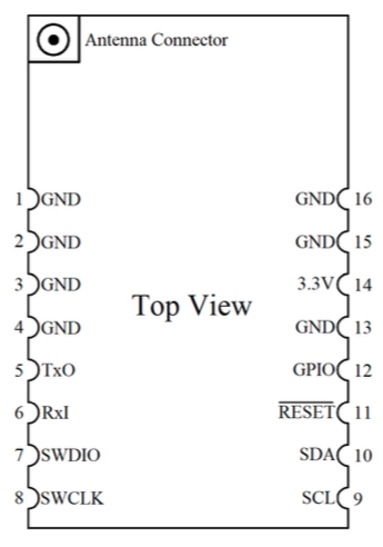
Haxiot provides templates for the PCB footprint in common formats such as Altium Designer and Autodesk EAGLE to assist in PCB layout and design of your LPWA end device product. A summary of the PCB layout requirements is shown below. Details on how the pinouts should be connected to your embedded device are here.
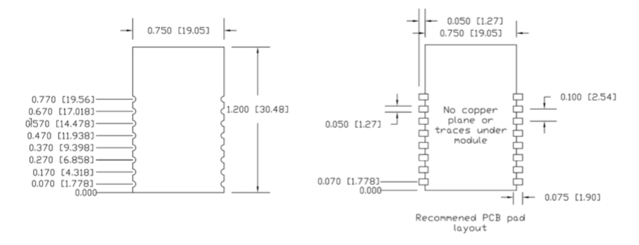
To create new shape files in other PCB layout applications, please refer to the HXC Client User Guide for footprint measurements. The 3D design can be downloaded from below.
Last updated:
Jan 01, 2024